Engineering Reference Guide · Semiconductor Packaging
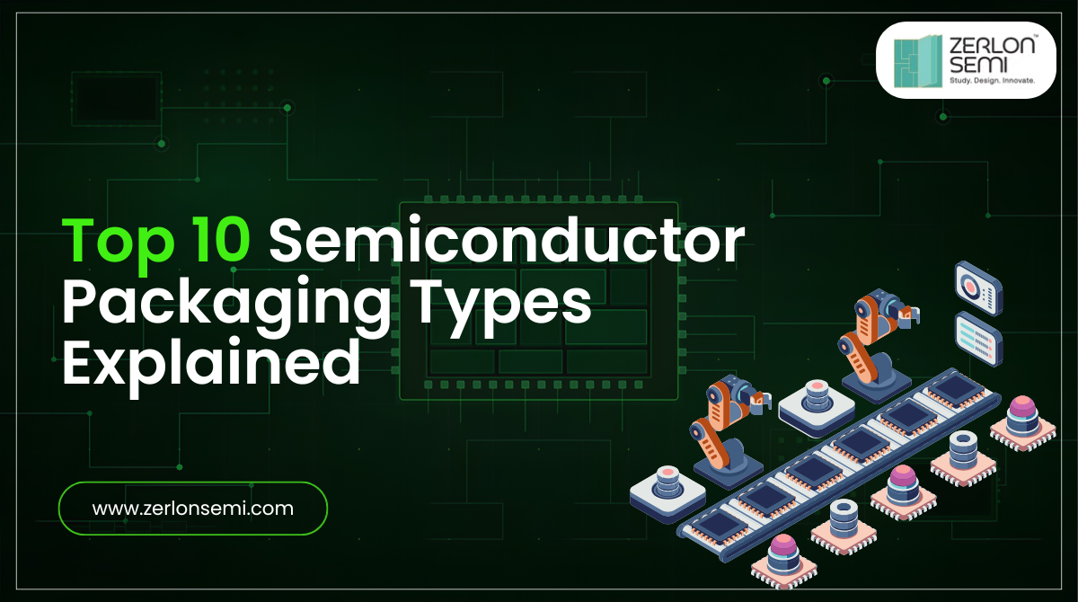
Top 10 Semiconductor Packaging Types Explained
DIP, QFP, QFN, BGA, Flip Chip, CSP, SOIC, LGA, SiP & WLP — what each one does, where it belongs, and how to choose.
What Is Semiconductor Packaging?
Semiconductor packaging is how a bare silicon chip gets turned into a component you can actually use on a circuit board. The package protects the die from moisture and physical damage, and provides the electrical connections to your PCB.
It’s not just a protective shell. The package you choose directly affects:
| Electrical Performance |
Longer leads = more inductance and capacitance. Bad for high-speed signals. |
| Heat Dissipation |
Exposed pads and metal slugs pull heat away from the die much faster. |
| Board Density |
Smaller packages let you pack more components into less space. |
| Rework & Testing |
Through-hole and gull-wing leads are easy to probe and hand-solder. BGA is not. |
| Manufacturing Cost |
Assembly complexity, inspection needs, and yield all factor into total cost. |
How to Choose the Right Package
Before locking in a package, evaluate these key factors:
| Pin Count |
How many I/O connections does the IC need? |
| Thermal Load |
How much heat does the device generate? Check θJA and θJC specs. |
| PCB Space |
Do you have room for gull-wing leads, or do you need a bottom-contact package? |
| Signal Frequency |
High-speed designs need short leads and low parasitic inductance. |
| Rework Needs |
Will a technician ever need to replace this part in the field? |
| App Grade |
Automotive and industrial have different reliability requirements than consumer. |
The Top 10 Semiconductor Packaging Types
01
DIP
Dual In-Line Package
| Description | The classic through-hole package with two rows of pins. Been around since the 1960s and still ships in the millions. Inserts into PCB holes or a breadboard socket. |
| Best for | Prototyping, education, legacy industrial systems, and any design where you need to hand-solder or replace components easily. |
| Watch out for | High pin counts, high-frequency circuits, or any design where board space is tight. |
02
QFP
Quad Flat Package
| Description | Gull-wing leads extend from all four sides. Surface-mount, no drilled holes needed. Common variants: LQFP (low-profile) and TQFP (thin). |
| Best for | Microcontrollers, FPGAs, DSPs. Popular in automotive ECUs where technicians need to visually inspect and rework solder joints. |
| Watch out for | Fine-pitch versions (0.4mm) demand very precise stencil printing during PCB assembly. |
03
QFN
Quad Flat No-Lead
| Description | No protruding leads — contacts are pads on the bottom perimeter. Most QFNs have a large central exposed pad (EP) for heat dumping. Very compact and electrically clean. |
| Best for | Power management ICs, RF chips, wireless SoCs, motor drivers. The ESP32 is a well-known QFN part. |
| Watch out for | Cannot visually inspect solder joints after reflow. X-ray inspection is required for quality assurance. |
04
BGA
Ball Grid Array
| Description | Solder balls on the entire underside enable huge pin counts in a compact footprint. Changed the industry for high-density, high-speed ICs. |
| Best for | Processors, memory (LPDDR, DDR), FPGAs, networking ASICs. Every laptop CPU is a BGA part. |
| Watch out for | Very difficult to rework without specialist equipment. Mandatory X-ray inspection. |
05
Flip Chip
Flip Chip Interconnect
| Description | The die is flipped face-down and connected directly to the substrate via solder bumps or copper pillars — no wire bonds. Extremely short electrical path. |
| Best for | High-performance processors, GPUs, RF amplifiers. Intel and AMD CPUs use flip-chip internally. |
| Watch out for | Requires specialist assembly equipment and processes. Not for general bench work. |
06
CSP
Chip Scale Package
| Description | By definition no larger than 1.2× the die area. Gets as close to bare silicon as possible while still packaged. Often under 1mm total height. |
| Best for | Smartphones, wearables, hearing aids, implantable medical devices — anywhere size is the primary constraint. |
| Watch out for | Fine-pitch contacts make rework extremely challenging without specialist tools. |
07
SOIC / SOP
Small Outline IC
| Description | A surface-mount version of DIP with gull-wing leads on two sides. Standard pitch 1.27mm. One of the most universally available SMT packages globally. |
| Best for | Op-amps, voltage regulators, logic ICs, EEPROM, interface chips. A go-to for prototyping with SMT parts. |
| Watch out for | Limited pin count compared to QFP or BGA. Not suitable for high-density or high-pin-count designs. |
08
LGA
Land Grid Array
| Description | Like BGA but without pre-attached solder balls. Flat land pads align to PCB pads. Socket-based LGA makes CPUs replaceable without soldering. |
| Best for | Desktop CPUs where upgradability matters (Intel LGA1700) and some RF/power applications. |
| Watch out for | Requires very precise PCB pad preparation. Socket variants add height and cost. |
09
SiP
System-in-Package
| Description | Multiple dies — logic, memory, RF, passives, MEMS — in one package. Not a single chip; a miniaturized system. Apple’s AirPods and Apple Watch use custom SiPs. |
| Best for | Wearables, IoT nodes, medical devices — anywhere you need a complete system in an extremely small footprint. |
| Watch out for | Custom SiP design is expensive. Typically only cost-effective at high volumes. |
10
WLP
Wafer-Level Package
| Description | Packaging happens at the wafer level before chips are cut apart. Result is a package exactly die-size — often under 0.5mm tall. Fan-out WLP extends I/O beyond the die edge. |
| Best for | Power management chips, RF transceivers, sensors, and baseband chips in smartphones. |
| Watch out for | Very fine-pitch connections make PCB design and assembly challenging. Requires advanced fabrication. |
Quick Comparison: All 10 Packages at a Glance
Use this table to quickly compare packages across the key selection criteria.
| Package |
Type |
Pin Count |
Rework |
Best Use Case |
| DIP | Through-hole | 4 – 64 | Very Easy | Prototyping, legacy systems |
| QFP | SMT perimeter | 32 – 256+ | Moderate | MCUs, FPGAs, automotive ECUs |
| QFN | SMT bottom | 4 – 100+ | Difficult | Power ICs, RF, wireless chips |
| BGA | SMT grid | 64 – 2000+ | Very Difficult | Processors, memory, FPGAs |
| Flip Chip | Die-level | 100s – 1000s | Specialist | GPUs, high-perf processors |
| CSP | SMT fine | Varies | Difficult | Mobile, wearables, medical |
| SOIC / SOP | SMT perimeter | 8 – 44 | Easy | Op-amps, regulators, logic |
| LGA | SMT / Socket | 100s – 1000s | Specialist | Desktop CPUs, RF |
| SiP | Multi-die | System-level | N/A | IoT, wearables, AirPods |
| WLP | Wafer-level | Varies | Difficult | Mobile PMICs, RF transceivers |
Key Takeaway:
DIP and SOIC are best for prototyping and low-frequency work. QFP gives the best balance of pin count and rework accessibility. QFN and BGA dominate high-performance designs. When miniaturization is everything, reach for CSP, WLP, or SiP.
Frequently Asked Questions
What is the most common semiconductor package?
SOIC and QFP are among the most common general-purpose SMT packages globally. BGA dominates in processors and memory. For new wireless and power designs, QFN is extremely popular.
What’s the difference between BGA and QFN?
Both have contacts on the bottom of the package, but BGA uses a full grid of solder balls across the entire underside — enabling hundreds to thousands of I/O. QFN uses flat pads only around the perimeter plus a central thermal pad. QFN suits lower pin counts with excellent thermal performance; BGA is for dense, high-I/O devices.
Which package is easiest to hand-solder?
DIP is the easiest — just insert into holes and solder. For SMT packages, SOIC (1.27mm pitch) is the most hand-solderable. QFP can be done with practice. QFN and BGA are not practical for hand soldering.
What does “exposed pad” mean on a QFN or DFN?
The exposed pad (EP) is a large metal pad on the bottom center of the package connected directly to the die’s thermal ground. Heat flows from the chip through the EP into your PCB copper pour. Always connect it to a copper pour with thermal vias for best performance.
What is the future of semiconductor packaging?
Advanced packaging is where much of the current innovation is happening. 2.5D packaging (multiple dies on a silicon interposer, like TSMC’s CoWoS used in Nvidia’s H100), 3D stacking, chiplet architectures, and fan-out wafer-level packaging are all growing rapidly — driven largely by AI hardware demands.
Ready to Build Your Career in Semiconductors?
Zerlon Semi
Specialized Semiconductor & VLSI Training | Coimbatore, India
Understanding semiconductor packaging is just the beginning. To truly master chip design — from RTL to silicon — you need hands-on training with the tools and methodologies used by the industry today. That’s exactly what Zerlon Semi delivers.
Built specifically for electronics and engineering graduates, Zerlon Semi is one of India’s leading specialized VLSI institutes — with a proven placement track record and a curriculum designed around what the semiconductor industry actually needs.
| What You Will Learn |
Career Outcomes |
- RTL Design & Verilog / VHDL
- SystemVerilog & UVM Verification
- FPGA Design & Implementation
- Semiconductor Packaging Fundamentals
- Industry-standard EDA Tools
|
- VLSI Design Engineer
- Verification Engineer
- FPGA / RTL Designer
- Semiconductor Test Engineer
- Roles at leading semiconductor MNCs
|
Why Zerlon Semi?
Industry-aligned curriculum · Proven placement record · Hands-on project training · Expert faculty from the semiconductor industry
Start your semiconductor career today: www.zerlonsemi.com