Physical Design Training — Floorplan to Tape-Out Certification Program
Master the complete Physical Design flow — Floorplanning, Placement, CTS, Routing, STA, DRC/LVS Signoff — using Cadence Innovus, Synopsys ICC2 and Mentor Calibre. The exact skills every PD engineer needs.
Core USPs of This Physical Design Program
Everything that makes Zerlon Semi's PD course the preferred choice for semiconductor layout engineers.
PD Course Overview
Master the complete Physical Design ASIC flow — from RTL netlist to GDS tape-out — covering floorplanning, power planning, placement, clock tree synthesis, routing, timing closure, and DRC/LVS signoff using Cadence Innovus, Synopsys ICC2 and Mentor Calibre.
PD Skills You Will Master
Skills demanded by every semiconductor company's PD hiring team — from India to global SoC companies.
Tools You Will Learn & Use
Production-licensed EDA tools — same as used at Qualcomm, Samsung and TSMC PD teams.
Offerings & Value of This PD Program
Every resource, tool and career support bundled into your enrollment — nothing hidden.
Physical Design Course Curriculum
Structured modules covering the complete PD flow — matching real hiring requirements at semiconductor companies.
Live Industry PD Projects
Portfolio-ready tape-out projects using production tools — exactly what PD interviewers want to see.
 Project 01Intermediate
 Project 02Advanced
 Project 03Expert
Register Now & Get Free Welcome Kit
Join India's top Physical Design training program — Innovus + ICC2 + Calibre by Zerlon Semi.
Why Choose Zerlon Semi's PD Course?
Why Choose Physical Design Engineering Now?
Who Should Do This PD Program?
Designed for ECE/EEE backgrounds — anyone wanting to enter semiconductor physical design roles.
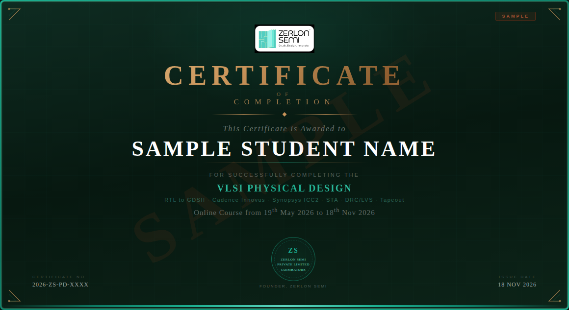
PD Expert Certification
Zerlon Semi Physical Design Expert Certificate — co-validated by 150+ semiconductor hiring partners.
What This Certificate Unlocks
What Can You Become?
Top career opportunities after completing the PD Expert certification at Zerlon Semi:
- Physical Design Engineer – Trainee
- ASIC Layout Engineer
- PnR Engineer – Entry Level
- Timing Analysis Engineer
- Senior PD Engineer
- PD Lead / Architect
- SoC Physical Integration Engineer
- Tape-Out Engineer
Physical Design Fee Structure
Flexible payment options — EMI at 0% interest. Enroll before 25 June 2025 for 10% early bird discount.
- Live Online Sessions
- Remote EDA Tool Access (Innovus/ICC2)
- 3 RTL-to-GDS Projects
- Lifetime Recordings
- PD eBook + Interview Q&A
- 5 Mock Interview Rounds
- Resume & LinkedIn Support
- Zerlon Semi PD Certificate
- Everything in Online +
- Weekend Offline Lab (Bangalore)
- Licensed EDA Tools On-Site
- In-Person PD Mentoring
- 10 Mock Interview Rounds
- Direct Company Referrals
- Calibre DRC/LVS Lab Access
- Lifetime Alumni Network
Simple Admission Process
Enrolled in under 48 hours — 4 simple steps.
Upcoming Batch Deadline
Our PD Alumni Work at Top Companies
2,000+ Zerlon Semi alumni placed across India's leading semiconductor companies.


Why Learners Choose Us Over the Rest
Dedicated Career Services by Zerlon Semi
We don't just train you — we stay with you until that PD offer letter is in your hands.
Success Stories from Our PD Learners

Testimonials from Our Students
Frequently Asked Questions
Start Your Physical Design
Career Today
Join 2,000+ engineers who chose Zerlon Semi to launch their semiconductor careers. Register now and get your Free Welcome Kit instantly.